

how PCB Clone applicate in electron field
2025-05-07
PCB (Printed Circuit Board) cloning in the electronics field refers to the process of duplicating an existing PCB design, either for repair, reverse engineering, or development purposes. Here’s how PCB cloning is applied in the electronics field:
Applications of PCB Cloning in Electronics
Reverse Engineering
Purpose: To understand how a competitor's product works or to replicate legacy electronics with no design files available.
Application: Engineers analyze the original PCB, trace its circuits, recreate the schematic, and then produce a new board.
Repair and Maintenance
Purpose: To restore function to discontinued or unsupported hardware.
Application: Clone damaged PCBs in industrial or military equipment to replace non-functional units.
Product Reproduction
Purpose: To mass-produce an existing PCB design.
Application: Small manufacturers or developers may clone a prototype into a manufacturable PCB for commercial use.
Upgrading and Modernizing
Purpose: To replace obsolete components with newer ones while keeping the original form factor.
Application: Cloning an old board and updating it to meet current standards, like adding USB instead of serial ports.
Educational and Learning Purposes
Purpose: To teach circuit design and reverse engineering.
Application: Students clone simple PCBs to learn how different components work together.
General PCB Cloning Process
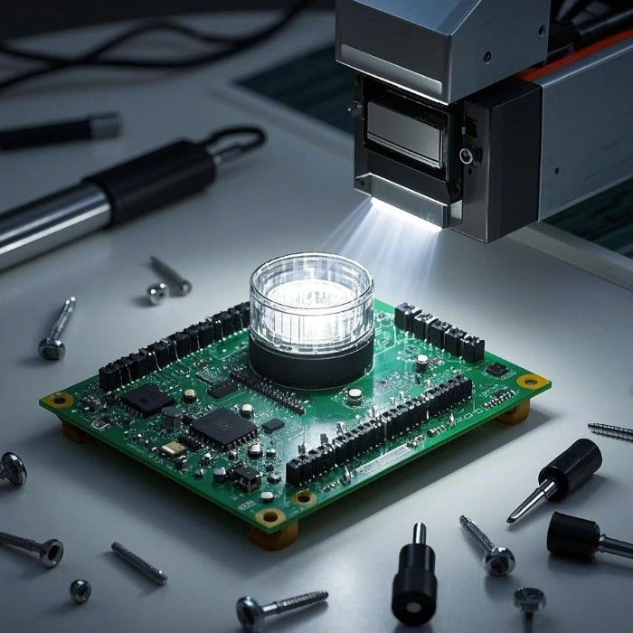
Physical Inspection and Imaging
Take high-resolution photos or scans of both sides of the PCB.
Schematic Extraction
Trace the connections manually or using software to recreate the schematic diagram.
PCB Layout Design
Redraw the board layout using EDA tools (like Altium, Eagle, or KiCad).
Component Identification
Identify and source the original or equivalent components.
Fabrication and Testing
Manufacture the new PCB and test it against the original to ensure functional accuracy.
If you are interested in our products or have any questions, please feel free to contact us and we will reply you within 24 hours.